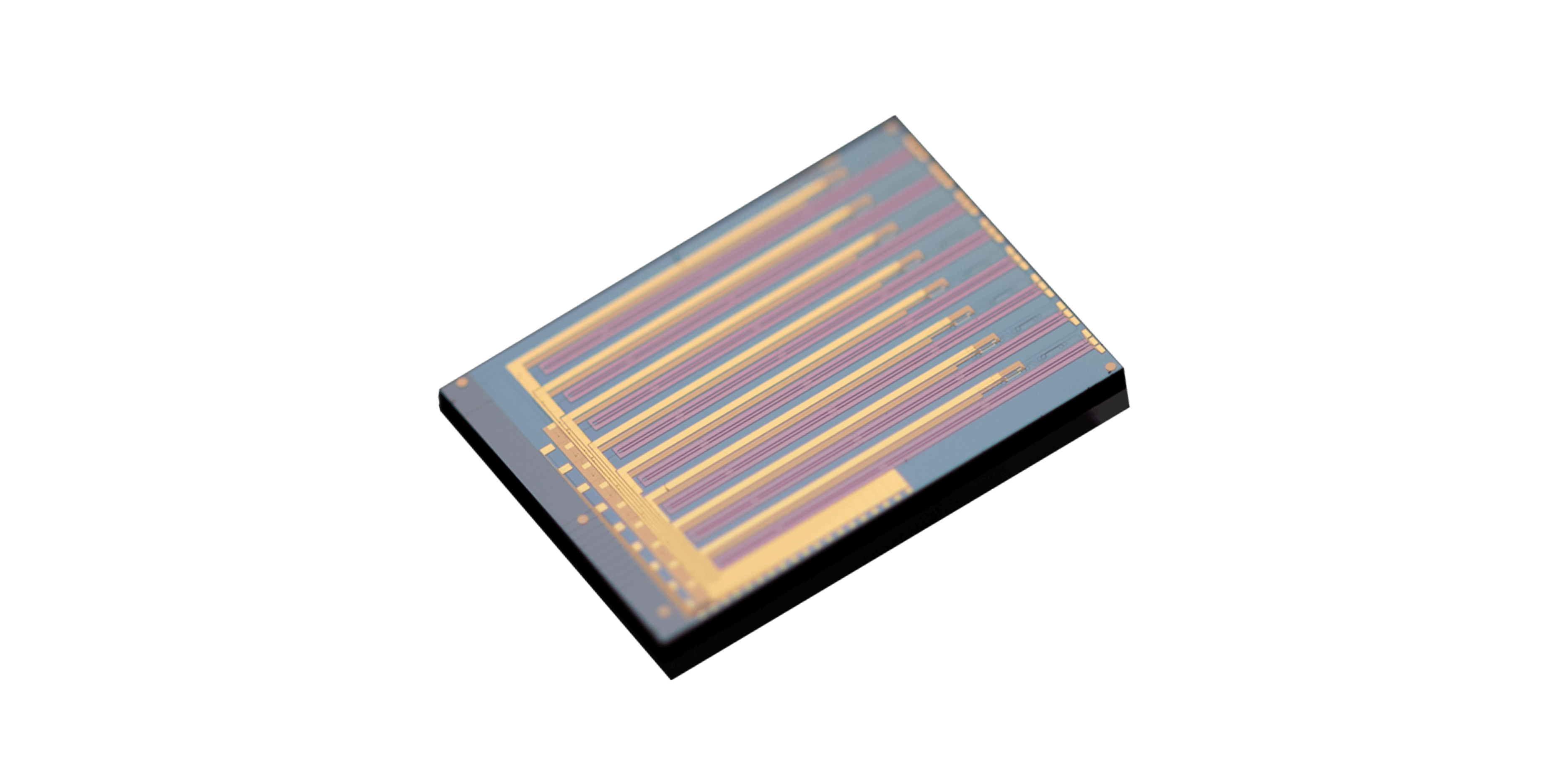
Thin-film lithium niobate has moved from a research material into a practical platform for high-speed optical modulation. They describe the technology by its function: an electric field changes the optical properties of a patterned lithium-niobate waveguide, allowing light intensity or phase to follow a data or measurement signal.
The thin film supports compact guiding and integrated electrodes. This definition matters because the same material can appear as a bare die, a multi-lane modulator, a coherent transmitter circuit, or a packaged device.
Each form transfers different responsibilities to the system developer. They therefore avoid asking whether the platform is “good” in isolation and instead examine what function is delivered at a specified reference plane. Current TFLN chips are published for data-center transceivers, coherent telecommunications, optical instruments, and sensing.
Their listed bandwidths range from 70 to 110 GHz, with product formats covering 800G through 3.2T. Those figures show the available direction, while a commercial design still requires detailed confirmation of wavelength, loss, voltage, packaging, reliability, and supply.
The Device Converts Electrical Information into Controlled Light
A TFLN photonic chip typically contains lithium-niobate waveguides and high-speed electrodes arranged to create an electro-optic modulator. In an intensity device, interferometric paths convert phase change into optical-power variation.
In an IQ circuit, nested structures control in-phase and quadrature components, enabling complex modulation that carries information in both amplitude and phase. The thin-film geometry lets TFLN chips combine strong electro-optic response with compact optical confinement. Published advantages include high bandwidth, low drive voltage, and low insertion loss relative to conventional approaches.
They treat these as measurable engineering objectives, not automatic outcomes, because electrode design, coupling, fabrication variation, and packaging determine how much of the material potential reaches the product. Important specifications describe different parts of the conversion.
Bandwidth indicates frequency response under stated conditions; half-wave voltage reflects the electrical drive needed for a defined phase shift; extinction ratio shows achievable optical contrast; insertion loss records optical power consumed. None alone predicts link performance, so they place them together in an electrical and optical system model.
Different System Architectures Use the Platform Differently
Direct-detection modules use multi-lane intensity-modulation products. A listed 1.6T DR8 or 800G DR4 device provides 70 GHz bandwidth, while a 3.2T DR8 version reaches 110 GHz. For these applications, the TFLN photonic chip must work with high-speed drivers, fiber arrays, receiver sensitivity, and thermal constraints inside dense data-center equipment.
Coherent transmission employs a different circuit. One 70 GHz PDMIQ product supports 800G and 1.6T ZR formats, combining polarization and IQ functions. Here, TFLN chips participate in generating complex optical fields that are recovered by coherent receivers and digital processing.
Bias stability, phase balance, optical loss, and driver linearity become central qualification concerns. Test and sensing developers may prefer a bare 110 GHz intensity-modulator die with lower listed loss at the chip reference plane.
This allows custom package, wavelength, and RF arrangements, but it also places coupling, hermeticity, reliability, and calibration work on the integrator. They select this route when the additional design freedom has a defined business and performance benefit.
Selection Depends on Interfaces, Evidence, and Production Responsibility
Their evaluation starts with an interface control document. For a TFLN photonic chip, it covers die dimensions, optical mode, coupling tolerance, pad geometry, impedance, bias access, permitted power, handling, and environmental limits. The document gives chip, package, driver, and module teams a common boundary and reduces late changes caused by incompatible assumptions.
Qualification of TFLN chips then proceeds through representative assemblies. They measure response, loss, voltage, extinction, temperature behavior, bias drift, and link error performance across several units and lots. Reliability tests are chosen for the intended environment.
A device for laboratory instrumentation may require different lifetime evidence from one installed in continuously operating network equipment. Commercial responsibility must be explicit. They determine who supplies known-good die, who owns coupling yield, how failures are analyzed, which process changes require approval, and what data accompany each shipment.
This allocation is particularly important for bare chips, where several companies may contribute to a final module and no single test captures all integration risks. Cross-functional education is useful during early adoption.
Packaging engineers, electronics designers, quality teams, and buyers may interpret the same chip specification differently. A shared review of reference planes, measurement methods, and responsibility boundaries reduces communication errors and makes technical negotiations faster and more precise. A clear definition turns an unfamiliar material acronym into a manageable component decision.
The platform is an electro-optic engine, but its practical value depends on the circuit format, package, electrical drive, optical budget, and verification plan around it. They use application requirements to select the implementation rather than forcing an existing device into every system.
Organizations considering the technology should begin with a small, instrumented prototype and a written qualification matrix. The prototype can reveal coupling sensitivity, driver margin, control needs, and test time before large commitments are made.
Those results also provide a factual basis for cost, volume, and roadmap discussions with suppliers and manufacturing partners. Clear responsibility at the supplier-integrator boundary reduces surprises during packaging and qualification. Samples from Liobate can be used to document coupling, RF, environmental, and lot behavior before assembly limits are finalized.
